Jaluino Cuckoo meets Arduino
In last post, Jaluino Cuckoo has been briefly exposed, at least this is what I have i mind… The idea is to “parasite” the Arduino and put an small board with a Microchip PIC microcontroller, instead off Atmel chip. Just like brood parasite cuckoo birds squat in other species nests.
Now it’s time to actually see how Jaluino Cuckoo could map Arduino pins. That is, we need to define which PIC’s pins are mapped with Arduino’s pins. This is an important step, as Atmel and Microchip chips are quite different, with different features, so a 100% mapping is hard to have, if not impossible. In the end, this is about making good compromises.
Overview of PIC18F25K22 features
In last post, PIC18F25K22 was chosen because it carries a lot of common features with Arduino, it has a lot of memory, runs fast, etc… Just to recall, Arduino provides:
- USART serial
- I²C amongst analog pins
- SPI
- 2 external interrupts
- 6 PWM channels
- 6 analog pins (or 4 if using I²C) and 1 voltage reference
- some other digital I/O pins
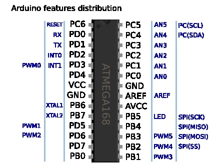
Now let’s see how 18F25K22 features are distributed amongst its pins:
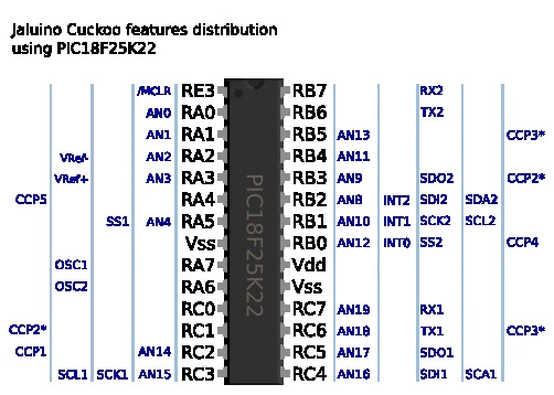
There are several advantages using PIC18F25K22. It has 2 USART, 2 MSSP for SPI and I²C, independent ANSEL-like analog pins, some PWM pins can be multiplexed in fuse. This means there’s a kind of flexibility while matching Arduino pins.
Tough pin mapping thoughts…
I started to match pin by features. Notations are A(p) for Arduino pin p, and J(p) for Jaluino pin p.
- power: A(VCC) = J(Vdd) or A(AVCC) = J(Vdd), A(GND left) = J(Vss left), A(GND right)= J(Vss right). GND pin mappings can be inverted.
- misc: A(RESET/PC6) = J(MCLR/RE3), A(XTAL1/PB6) = J(OSC1/RA7), A(XTAL2/PB7) = J(OSC2/RA6). XTAL pin mappings can be inverted
- serial: TX1 pin also carries CCP3 PWM output. RX2/TX2 don’t carry anything than USART module #2, so we’ll match A(RX/PD0) = J(RX2/RB7) and A(TX/PD1) = J(TX2/RB6).
- SPI: Arduino SPI is tricky as SS pin also carry PWM4 and MOSI also carry PWM5. This means, on Jaluino, we need to find pin with the same carried features. There’s none… So this basically means we have to sacrifice 2 PWM channels in favor of SPI. Now which SPI module to choose ? SPI#2 pins on 18f25K22 also carry 3 external interrupts and 1 PWM outputs, and I consider external interrupts as important, so mapping will use SPI#2. Assuming MISO equivalent to SDO and MOSI equivalent to SDI, A(SCK/PB5) = J(SCK1/RC3),A(MISO/PB4) = J(SDO1/RC5), A(MOSI/PB3) = J(SDI1/RC4) and A(SS/PB2) = J(SS1/RA5). Note SPI#1 pins aren’t closed together, this may be a problem while designing the PCB.
- I²C: since we mapped SPI using MSSP#1, I²C will use MSSP#2. A(SCL/PC5) = J(SCL2/RB1), A(SDA/PC4) = J(SDA2/RB2)
- Interrupts: this is a tough part, again compromise ahead… Consequence of SPI and I²C mapping: 18F25K22 INT1 and INT2 interrupt pins are shared with I²C pins. In Arduino, I²C pins don’t carry interrupts. Again, we’re loosing 1 interrupt ! The only remaining interrupt on Jaluino is INT0. Arduino INT1 also carries a PWM signal, same for INT0 on Jaluino. So let’s match Jaluino INT0 with Arduino INT1: A(INT1/PD3) = J(INT0/RB0).
- PWM: from 18F25K22 datasheet, I understand there are 2 standard CPP and 3 enhanced ECCP modules. I also understand this can produce up to 5 PWM channels. And I finally also understand some are multiplexed (CCP2* and CCP3*). We’ve already mapped A(PWM0) as it’s also involved in interupts. We’ve also lost 2 PWM channels because of SPI mapping. On Arduino, MOSI/PB3 also carry PWM5 and we mapped it to RC4, which doesn’t have PWM. Same for PWM4/SS. So, remaining PWM channels can go as: A(PWM1/PD5) = J(CCP1/RC2), A(PWM2/PD6) = J(CCP2*/RC1), A(PWM3/PB1) = J(CCP3*/RB5).
- Digital I/O: there are 4 remaining digital I/O pin to map, why not A(PD4) = J(RC0), A(PD7) = J(RC7), A(PB0) = J(RC6). Note: two out of these can be used as another serial connection, an added feature coming with Cuckoo. Finally, we’ve lost an interrupt but we can map a PWM pin instead (not compatible, but a consolation. A(INT0/PD2) = J(CCP2*/RB3)
- Analogs: finally, there are 4 remaining analog inputs. There are several possibilities since there are independent in 18F25K22 (can be configured independently from each other). Let’s map A(AN3/PC3) = J(AN11/RB4), A(AN2/PC2) = J(AN0/RA0), A(AN1/PC1) = J(AN1/RA1), A(AN0/PC0) = J(AN0/RA0).
Phew…
Let’s sum up this in the following table:
| . | Arduino | Jaluino Cuckoo | Comments |
| Power | VCC | Vdd | AVCC can also be mapped with Vdd |
| GNDleft | Vssleft | GND left/right can be inverted | |
| GNDright | Vssright | ||
| Misc | RESET/PC6 | MCLR/RE3 | |
| XTAL1/PB6 | OSC1/RA7 | XTAL can be inverted as needed | |
| XTAL2/PB7 | OSC2/RA6 | ||
| Serial | RX/PD0 | RX2/RB7 | |
| TX/PD1 | TX2/RB6 | ||
| SPI | SCK/PB5 | SCK1/RC3 | |
| MISO/PB4 | SDO1/RC5 | ||
| MOSI/PB3 | SDI1/RC4 | ||
| SS/PB2 | SS1/RA5 | ||
| I²C | SCL/PC5 | SCL2/RB1 | |
| SDA/PC4 | SDA2/RB2 | ||
| Interrupts | INT1/PD3 | INT0/RB0 | this is also PWM0 |
| PWM | PWM1/PD5 | CCP1/RC2 | |
| PWM2/PD6 | CCP2*/RC1 | multiplexed with CCP2*/RB3 (PWM5) | |
| PWM3/PB1 | CCP3*/RB5 | ||
| Digital I/O | PD4 | RC0 | these are the remaining ones… |
| PD7 | RC7 | ||
| PB0 | RC6 | ||
| INT0/PD2 | CCP2*/RB3 | ||
| Analog inputs | AN3/PC3 | AN11/RB4 | remaining ones… |
| AN2/PC2 | AN0/RA0 | ||
| AN1/PC1 | AN1/RA1 | ||
| AN0/PC0 | AN2/RA2 | ||
| AREF | Vref+/RA3 | ||
| Extra | PWM5/MOSI/PB3PWM4/SS/PB2 | CCP5/RA4 | using jumper ? |
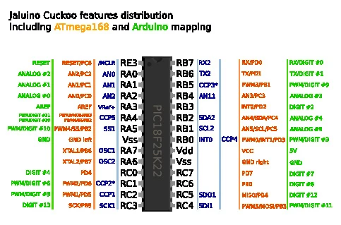
This diagram may sum up this even better:
Limitations
Despite the great number of features brought by PIC18F25K22, we’ve lost a lot of them during this mapping:
- 2 PWM outpus were sacrificed, PWM4 on DIGIT#10 and PWM5 onDIGIT#11. This pins can only be used as simple digital ones.
- 1 interrupt was also discarded, INT0 on DIGIT#2.
Next steps ?
Schematic, PCB design, tests, failures, iterate…